|
home /
infca /
pic452
(navigation links)
|
"Deixar una cosa per a demà és deixar-la per sempre més".
Josep Pla
|
El PIC 18F452
 This powerful 10 MIPS (100 nanosecond instruction execution)
yet easy-to-program (only 77 single word instructions)
CMOS FLASH-based 8-bit microcontroller
packs Microchip's powerful PIC architecture
into an 40- or 44-pin package
and is upwards compatible with the PIC16C5X, PIC12CXXX, PIC16CXX and PIC17CXX devices
and thus providing a seamless migration path of software code
to higher levels of hardware integration.
This powerful 10 MIPS (100 nanosecond instruction execution)
yet easy-to-program (only 77 single word instructions)
CMOS FLASH-based 8-bit microcontroller
packs Microchip's powerful PIC architecture
into an 40- or 44-pin package
and is upwards compatible with the PIC16C5X, PIC12CXXX, PIC16CXX and PIC17CXX devices
and thus providing a seamless migration path of software code
to higher levels of hardware integration.
The PIC18F452 features a 'C' compiler friendly development environment,
256 bytes of EEPROM, Self-programming, an ICD,
2 capture/compare/PWM functions,
8 channels of 10-bit Analog-to-Digital (A/D) converter,
the synchronous serial port can be configured as either
3-wire Serial Peripheral Interface (SPIT)
or the 2-wire Inter-Integrated Circuit (ICT) bus
and Addressable Universal Asynchronous Receiver Transmitter (AUSART).
All of these features make it ideal for
manufacturing equipment, instrumentation and monitoring, data acquisition,
power conditioning, environmental monitoring, telecom
and consumer audio/video applications.
(April 2008) The PIC18F452 its obsolete.
There is a very good 16F guide
here
and the 16F877 is pin compatible.
Better use 18F4620 .
Arquitectura
| Registre | Funció | Detalls
|
| WREG | working register |
|
| INTCON | control d'interrupcions | 0=disabled, 1 = enabled (see INTCON)
|
| T1CON | control del timer 1 | load preset value (?)
|
| TMR1H&L | | (?)
|
| WDTCON | watch dog control | (?)
|
| PORTB | reads the pin levels / write to the port latch
| input/output
|
| LATB | output latch | output
|
| TRISB | data direction | 1=input, 0=output
|
Each port has three registers for its operation.
These registers are:
- TRIS register (data direction register)
- PORT register (reads the levels on the pins of the device)
- LAT register (output latch)
The data latch (LAT register) is useful
for read-modifywrite operations on the value
that the I/O pins are driving.
Reading the PORTx register reads the status of the pins,
whereas writing to it will write to the port latch.
PORTA is a 7-bit wide, bi-directional port.
PORTB is an 8-bit wide, bi-directional port.
PORTC is an 8-bit wide, bi-directional port.
PORTD is an 8-bit wide, bi-directional port.
PORTE is a 3-bit wide, bi-directional port.
Features
| Operating frequency | DC-40 MHz
|
| Program memory (bytes) | 32 K (0..0x7FFF)
|
| Data memory (bytes) | 1536 (0..0x5FF)
|
| Data EEPROM memory (bytes) | 256
|
| I/O ports | A thru E (5)
|
| Timers | 4
|
| 10-bit AtoD module | 8 input channels
|
| Instruction set | 75 instructions
|
Registers - program counter (PCL), STATUS, working (WREG),
bank select register (BSR), mapped ports (TRISx),
interrupt control (INTCON), file select (FSR#), special function (SFR).
Memory organization
|
The Special Function Registers (SFRs) are registers
used by the CPU and Peripheral Modules
for controlling the desired operation of the device.
These registers are implemented as static RAM,
from 0xF80 thru 0xFFF (up to 128SFRs).
|

|
Oscillator modes
|
The PIC18FXX2 can be operated in eight different Oscillator modes.
The user can program three configuration bits (FOSC2, FOSC1, and FOSC0)
to select one of these eight modes:
- 1. LP Low Power Crystal
- 2. XT Crystal/Resonator
- 3. HS High Speed Crystal/Resonator
- 4. HS + PLL High Speed Crystal/Resonator with PLL enabled
- 5. RC External Resistor/Capacitor
- 6. RCIO External Resistor/Capacitor with I/O pin enabled
- 7. EC External Clock
- 8. ECIO External Clock with I/O pin enabled
In XT, LP, HS or HS+PLL Oscillator modes,
a crystal or ceramic resonator
is connected to the OSC1 and OSC2 pins to establish oscillation.
Atenció : seleccionem XT mode, 4 MHz crystal, C1 = C2 = 22 pF.
For RCIO oscilator configuration, the values are :
100K > R(ext) > 3K ;
C(ext) > 20pF
Page 294, Bibl-3 : Vdd=5,0 v, C=20pF, R=3K3 => F(osc)=3,5 MHz.
|

|
Configuration bits
There are several features intended to maximize system reliability,
minimize cost through elimination of external components,
provide power saving Operating modes and offer code protection.
The configuration bits can be programmed (read as '0'),
or left unprogrammed (read as '1'), to select various device configurations.
These bits are mapped starting at program memory location 300000h.
The user will note that address 300000h
is beyond the user program memory space.
In fact, it belongs to the configuration memory space (300000h - 3FFFFFh),
which can only be accessed using Table Reads and Table Writes.
The sequence of events for programming configuration registers is:
- Load table pointer with address of configuration register being written.
- Write a single byte using the TBLWT instruction.
- Set EEPGD to point to program memory,
set the CFGS bit to access configuration registers,
and set WREN to enable byte writes.
- Disable interrupts.
- Write 55h to EECON2.
- Write AAh to EECON2.
- Set the WR bit. This will begin the write cycle.
- CPU will stall for duration of write
(approximately 2 ms using internal timer).
- Execute a NOP.
- Re-enable interrupts.
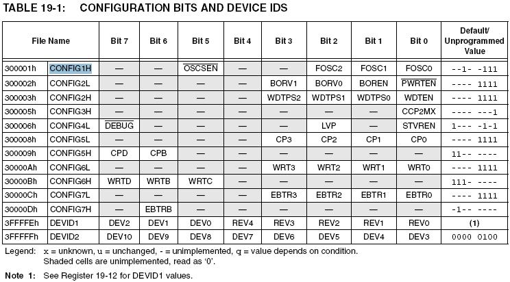
- CONFIG1H
bit 7 bit 0
.---------.---------.---------.---------.---------.---------.---------.---------.
| --- | --- | OSCSEN/ | --- | --- | FOSC2 | FOSC1 | FOSC0 |
.---------.---------.---------.---------.---------.---------.---------.---------.
- bit 5 = Oscilator System Clock Switch Enable
1 = disables "oscilator system clock switch" option ;
0 = oscilator switching is enabled.
- bits2:0 : Oscilator Selection bits :
- 111 = RC oscillator with OSC2 configured as RA6 [*]
- 110 = HS oscillator with PLL enabled
- 101 = EC oscillator with OSC2 as RA6
- 100 = EC oscillator with OSC2 as divide-by-4 clock output
- 011 = RC oscillator
- 010 = HS oscillator
- 001 = XT oscillator
- 000 = LP oscillator
[*] Default (unprogrammed) value := 0b--1- -111 ;
Atenció : s'ha de programar a 0b0010.0001, x'21, modus "XT" ;
MPLAB IDE v8.0 : Configure + Configuration bits.
See "Setup"
To configure the PIC with the oscilation mode you decide to use,
you may setup correctly the "Configuration bits".
That is, if you use MPLAB environment,
on "Configure" main menu, the "Configuration Bits..." option.
However, if you not use MPLAB,
you can setup the configuration bits by code: see page 197 of PIC18F452 DS.
url
En ensamblador :
// Para cambiar CONFIG1H, direccion = 0x300001
MOVLW 30
MOVWF TBLPTRU
MOVLW 00
MOVWF TBLPTRH
MOVLW 01
MOVWF TBLPTRL
MOVLW B'XXXXXXXX' // NUEVA CONFIGURACION
Main Registers
- INTCON
bit 7 bit 0
.---------.---------.---------.---------.---------.---------.---------.---------.
| GIE | PEIE | TMR0IE | RBIE | GIE | TMR0IF | INT0IF | RBIF |
.---------.---------.---------.---------.---------.---------.---------.---------.
- bit 7 = Global Interrupt Enable.
1 = enables all unmasked interrupts.
0 = disables all interrupts.
- bit 6 = Peripheral Interrupt Enable.
1 = enables all unmasked peripheral interrupts.
0 = disables all peripheral interrupts.
- bit 5 = Timer0 Overflow Interrupt Enable.
1 = enables the TMR0 overflow interrupt.
0 = disables the TMR0 overflow interrupt.
- bit 4 = External Interrupt Enable.
1 = enables the INT0 external interrupt.
0 = disables the INT0 external interrupt.
- bit 3 = RB Port Change Interrupt Enable.
1 = enables the RB port change interrupt.
0 = disables the RB port change interrupt.
- bit 2 = TMR0IF Overflow Interrupt Flag.
1 = TMR0 register has overflowed (must be cleared in soft).
0 = TMR0 register did not overflow.
- bit 1 = INT0IF : INT0 External Interrupt Flag.
1 = INT0 external interrupt occurred (must be cleared in soft).
0 = external interrupt did not occur.
- bit 0 = RBIF : RB Port Change Interrupt Flag.
1 = at least one of the RB7:RB4 pins changed state (must be cleared in soft).
0 = none of the RB7:RB4 pins have changed state.
- ADCON0
bit 7 bit 0
.---------.---------.---------.---------.---------.---------.---------.---------.
| ADCS1 | ADCS0 | CHS2 | CHS1 | CHS0 | GO/-DON | - | ADON |
.---------.---------.---------.---------.---------.---------.---------.---------.
- bit 7-6 = A/D conversion clock select bits 1 and 0.
- bits 5-3 = Analog channel select bits.
- bit 2 = A/D conversion status
1 = A/D conversion in progress
0 = A/D conversion not in progress
- bit 0 = A/D on bit
1 = A/D converter module is powered up
0 = A/D converter module is shut-off
- ADCON1
bit 7 bit 0
.---------.---------.---------.---------.---------.---------.---------.---------.
| ADFM | ADCS2 | - | - | PCFG3 | PCFG2 | PCFG1 | PCFG0 |
.---------.---------.---------.---------.---------.---------.---------.---------.
- bit 7 = A/D result format select bit
1 = right justified. 6 most significant bits of ADRESH are '0'.
0 = left justified. 6 least significant bits of ADRESL are '0'.
- bit 6 = A/D conversion clock select bit 2.
- bits 3-0 = A/D port configuration control bits.
Instruction set
| Mnemonic | Meaning
|
| BCF | bit Clear
|
| BSF | bit Set
|
| BTFSC | bit test, skip if Clear
|
| BTFSS | bit test, skip if Set
|
| CLRF | clear f
|
| DECF | decrement f
|
| DECFSZ | decrement, skip is zero
|
| INCF | increment f
|
| MOVF | move f
|
| MOVFF | move fs to fd
|
| MOVLW | move literal to register W
|
| MOVWF | move WREG to f
|
| SETF | set f
|
Timer control
Timer0 can operate as a timer or as a counter.
The TMR0 interrupt is generated
when the TMR0 register overflows from FFh to 00h in 8-bit mode,
or FFFFh to 0000h in 16-bit mode.
Timer mode is selected by clearing the T0CS bit.
In Timer mode, the Timer0 module will increment
every instruction cycle (without prescaler).
Counter mode is selected by setting the T0CS bit.
In Counter mode, Timer0 will increment,
either on every rising or falling edge of pin RA4/T0CKI.
Registers associated with Timer0 :
- TMR0L - timer0 Module Low byte register.
- TMR0H - timer0 Module High byte register.
- INTCON
- T0CON
- (7) TMR0ON - Timer0 On/Off Control bit. 1 = enables Timer0; 0 = stops Timer0.
- (6) T08BIT - Timer0 8-bit/16-bit Control bit. 1 = Timer0 is a 8-bit timer/counter; 0 = 16-bit.
- (5) T0CS - Timer0 Clock Source Select bit. 1 = transition on T0CKI pin; 0 = internal instruction cycle.
- (4) T0SE - Timer0 Source Edge Select bit. 1 = high-to-low; 0 = low-to-high.
- (3) PSA - Timer0 Prescaler Assignement bit. 1 = Timer1 prescaler NOT asigned; 0 = prescaler assigned.
- (2) T0PS2 - Timer0 Prescaler Select bits :
- (1) T0PS1 - 000 = 1:2 prescale, 001 = 1:4, 010 = 1:8, 011 = 1:16,
- (0) T0PS0 - 100 = 1:16, 101 = 1:64, 110 = 1:128, 111 = 1/256 prescale value.
Set Timer 0 : set TMR0HyL + set INTCON + start Timer0.
Stop Timer 0 : T0CON := 0x00 ; (7) disable.
Start Timer 0 : T0CON := 0xC8 ; (7) enable, (6) 8-bit, (3) no prescaler.
Resum de la configuració
CONFIG1H := 0b0010.0001 ; // XT mode
Port "A" :
CLRF PORTA ; Initialize PORTA by clearing output data latches
CLRF LATA ; Alternate method to clear output data latches
MOVLW 0x07 ; Configure A/D
MOVWF ADCON1 ; for digital inputs
MOVLW 0xCF ; Value used to initialize data direction
MOVWF TRISA ; Set RA<3:0> as inputs ; RA<5:4> as outputs
ADCON1 := 0b0000.1110 ; // ADFM=0(bit7) => left justify ADRESH+L, PCFG=1110(bits3-0) => AN0 analog, Vref=Vdd;
.
.
Una configuració mínima de HW és doncs :

|
ADC
The ADRESH and ADRESL registers contain
the (10-bit) result of the A/D conversion.
This register pair is 16-bits wide.
If ADFM=1 then it is Right justified.
If ADFM=0 then it is Left justified.
When the A/D conversion is complete,
the result is loaded into the ADRESH/ ADRESL registers,
the GO/DONE bit (ADCON0<2>) is cleared,
and A/D interrupt flag bit, ADIF is set.
The ADCON1, TRISA and TRISE registers
control the operation of the A/D port pins.
The port pins that are desired as analog inputs,
must have their corresponding TRIS bits set (input).
The following steps should be followed for doing an A/D conversion:
- Configure the A/D module:
- Configure analog pins, voltage reference and digital I/O (ADCON1)
- Select A/D input channel (ADCON0)
- Select A/D conversion clock (ADCON0)
- Turn on A/D module (ADCON0)
- Configure A/D interrupt (if desired):
- Clear ADIF bit
- Set ADIE bit
- Set GIE bit
- Set PEIE bit
- Wait the required acquisition time.
- Start conversion:
- Wait for A/D conversion to complete, by either:
- Polling for the GO/DONE bit to be cleared
(interrupts disabled)
OR
- Waiting for the A/D interrupt
- Read A/D Result registers (ADRESH/ADRESL);
clear bit ADIF if required.
- For next conversion, go to step 1 or step 2 as required.
[Bibl-3], chapter 17.
A/D conversion code
sample.
Al utilizar un periférico, no importa de que microcontrolador,
lo recomendable es atenerse a las banderas de estado o status.
En el registro ADCON0, el bit 2 es llamado "GO/-DONE".
Se usa para arrancar, pero también indica el estado.
Escribes un uno para arrancar la conversión,
y mientras permanece en uno, el convertidor está trabajando.
Al momento que la conversión termina, el bit "GO/-DONE" cae a cero.
Eso está en la hoja de datos del microcontrolador.
Para no desperdiciar ciclos,
es preferible usar una rutina de interrupción de fin de conversión.
.
.
Detallets
The PIC18FXX2 oscillator design requires the use
of a parallel cut crystal.
[Bibl-1]
Sample code is in the 18F452 datasheet.
After battling with a 18F452 for ages,
trying to get it to run at 40 MHz using the PLL_HS with a 10 MHz resinator,
all I could get it to do was oscilate at 10 MHz.
The solution is to add a 4M7 resistor across the osc1 and osc2 pins.
Works like a charm!
url
Each ADC needs a reference voltage which defines 100% or 0xFF (for a 8-Bit ADC).
In the case of your PIC
there is a matrix in the
datasheet
on page 184, chapter 17.
ICSP
| pin name | pin | type | description
|
| MCLR/Vpp/RE3 | 1 | power | programming enable
|
| Vdd | 11, 32 | power | power supply
|
| Vss | 12, 31 | power | ground
|
| RB5/PGM | 38 | input | low voltage input
|
| RB6/PGC | 39 | input | serial clock
|
| RB7/PGD | 40 | input | serial data
|
In this mode, the RB5/PGM pin is dedicated to the programming function
and ceases to be a general purpose I/O pin.
The trade off is, if LVP is enabled, PGM pin cannot be used as I/O anymore.
During programming, VDD is applied to the MCLR/VPP pin.
To enter Programming mode, VDD must be applied to the RB5/PGM,
provided the LVP bit is set.
While in low voltage ICSP mode,
the RB5 (PGM, pin 38) pin can no longer be used as a general purpose I/O pin,
and should be held low during normal operation
to protect against inadvertent ICSP mode entry.
Vpp = High voltage ICSP programming enable pin.
MCLR = Master Clear (Reset) input.
This pin is an active low RESET to the device.
The LVP bit defaults to a ('1') from the factory.
19.8, Low Voltage ICSP Programming, DS39564C-page 210 [212/332]
PGM = Low Voltage ICSP programming enable pin.
PGC = In-Circuit Debugger and ICSP programming clock pin.
PGD = In-Circuit Debugger and ICSP programming data pin.
LVP - programador per al 18F452
|
For reading and writing program memory using this adapter,
you also have to apply power to the PIC (+5V at Vdd)
and tie MCLR to high level (Vdd);
Microchip suggests to use a resistor for MCLR because of latch-up risk.
An oscillator circuit doesn't have to be connected.
Of course, connect the three lines PGD, PGC and PGM to this adapter, too.
Since you use Low Voltage Programming-mode,
pin PGM (38 = RB5/PGM) is not usable for I/O.
If you programm a PIC in this manner,
always ensure PGM is pulled low in the application
(e.g. by adding 10K to ground)
even if the schematics look different.
Otherwise the PIC might enter programming mode instead of normal working mode.
LVP-mode is enabled by high level on pin PGM.
The second 10k resistor at PGM pulls this pin to ground
if no PC is connected
and thus safely prevents the PIC from entering LVP-mode.
Don't high voltages on RS-232 harm the PIC?
All the PIC's I/O-pins are protected against electric discharge
by internal diodes to Vss and Vdd (see datasheet!).
With a resistor limiting the pin current,
all voltages will get clamped between 0V and 5V.
For programming, you can use
ICProg from Bonny Gijzen.
Configure as JDM-type-programmer ...
(JDM homepage)
|

D-9 :
pin3 = TxD,
pin 4 = DTR,
pin 5 = GND,
pin 7 = RTS,
pin 8 = CTS.
PIC :
PGD = pin 40,
PGC = pin 39,
PGM = pin 38.
MCLR = pin1 [Vih := Vdd + 4v]
Vdd (+) = pin 11 i 32.
Vss (-) = pin 12 i 31.
|

|
Before building this programmer,
be sure that your serial port (RS232) have at least 11 Volts.
needed to program the Series "C" (12C50X, 16C84, etc).
With 9.5 volts you will be able to program only a few microcontrollers.
If you get an error while programming,
change the 1mF capacitor to 0,47mF.
Doesn't work?
Maybe the voltage at the port is not good enough.
Put a 10mF capacitor between the VDD and GND.
|

Melting mr's Lothar
design (up right)
with mr's Jose Pino
design (up left),
here you have a working LVP for 18F452 !
Que fa el IC-prog ? What does IC-prog ?
Posa TxD (pin 3/9 x PGM and "delayed" x MCLR) a "ON".
RTS (pin 7/9 x PGC) i DTR (pin 4/9 x PGD) estan alternant {as Data and Clock}
Atenció :
per programar el PIC, s'ha de
-
posar el cable des R(27ohms) al Pin1 del PIC
- treure el cristall
- ( no fer servir "RS232 check tester" )
Per ejecutar el PIC, aquestes mesures s'han de invertir, es clar ...
Mesures del RS-232 :
| Equip | Voltatge TxD & RTS
| | Kayak | 9,1 volts.
| | P4 | 10 volts.
| | RAP | 10,5 volts.
| | P90 | 10,0 volts.
| | PC-330 | 9,7 volts.
| | PCI port | ?
|
Poso IC-prog a P4/RAP => "File + Open" tanca el programa !?
c:> ic-prog.exe -lFILENAME.HEX -p
|
IC-Lab problems win XP
Símptomes :
"Privileged instruction",
"Access violation ...",
- Src :
url [582447 bytes]
- get ICprog.sys -
url [5248 bytes]
- place it where ICprog.exe is
- ICprog.exe properties + Compatibility +
"Run this program in compatibility mode for" : "Windows 2000".
- ICprog + Settings + Options + "Misc" : "Enable NT/2000/XP driver".
P4 - mola {21-09-2008} !
MPLAB Tools v 8.00
-
8-bit MCU's : PIC10x, PIC12x, PIC16x, PIC17x, PIC18x and rfPIC devices.
-
16-bit MCU's : dsPIC30x, dsPIC33, PIC24x.
-
32-bit MCU's : PIC32 devices.
Install :
- 8-bit MCUs
- uChip Applications :
- MPASM = MPASM + MPLINK + MPLIB.
- MPLAB C32 = ASM32, LINK32, C32 C compiler y Utilities.
- MPLAB IDE :
- AN851 = FLASH Bootloader
- MPLAB ICD 2 = in-circuit debugger
- MPLAB SIM = simulator
- MPLAB IDE Tools :
- Data Monitor and Control Interface
New Project :
- device := 18F452 ;
- toolsuite := MPASM ;
- path := d:\Projects\ ;
url
Few basic ASM programs
list p=16f452
#include p18f452.inc
Dest equ 0x0B ; define constant
org 0x0000 ; Reset vector
goto Start ; skip interrupt vectors
org 0x0100 ; user program start
Start
movlw 0x0A
movwf Dest ;
bcf Dest,3 ;
goto Start ; loop
end
A more interesting one :
title "PIC18F452 counting program"
list p=18f452,f=inhx32
#include <p18f452.inc> ; This "header file" contains all the PIC18F252 special function register names and addresses.
; This file is located in the same directory as MPASMWIN.EXE.
COUNT equ 0x00
DVAR equ 0x01
DVAR2 equ 0x02
org 00h ; reset vector
goto Start
org 1Ch
Start
clrf WREG ; clear W register
movwf PORTC ; clear PORTC
movwf TRISC ; config PORTC as outputs
Init
clrf COUNT ; clr count
IncCount
incf COUNT,F ; increment count
movf COUNT,W ;
movwf PORTC ; display on port c
call Delay ; wait
goto IncCount ; loop
;
Delay
movlw 0xFF ; set delay loop
movwf DVAR2 ;
D0
movwf DVAR ; reset inner loop
D1
decfsz DVAR,F
goto D1
decfsz DVAR2,F
goto D0
return
end
[Bibl-4]
A simple program fragment that reads a string of fixed characters is:
movlw low string ; get low byte of string address
movwf TBLPTRL ; set the low byte of pointer
movlw high string ; repeat for high byte
movwf TBLPTRH
nextchar
tabrd * ; moves char to TABLAT
movf TABLAT,W ; test for null char
btfsc STATUS,Z ; ANSI string delimiter
goto endofstring
call LCD_CHAR ; do the display part
incf TBLPTRL
btfsc STATUS,C ; remember to check for overflow
incf TBLPTRH
goto nextchar
endofstring
url
The data strings are stored in memory like this :
DB 't', 0x55, '\n', 0x00 ; 8-bit data.
DT "Version 1.2a, 22/04/2008." ; RETLW 8-bit.
An improved sample, from MicroChip :
table.zip
Few interesting Macros
int_off MACRO ; disables all interrupts
bcf intcon,gie
btfsc intcon,gie ; make sure bit cleared (int could have occurred 1/2way thru instruction)
goto $-2
ENDM
int_on MACRO ; re-enable interrupts
bsf intcon,gie
ENDM
url
Few Tips & Tricks
For relocatable code, use UDATA to create a data (RAM) section.
For absolute code, use EQU or CBLOCK.
Add 18F452.LKR file to the "project-name" Linker folder.
Otherwise MPLINK is not invoqued, and no .map file generated.
First Things First
- Flashing LED.
16F877 sample.
Disco Fever (0x09 @ 18F452).
Codi (20/04/2008) :
UNO.ASM
- 7-segment sequence.
Codi (27/04/2008) :
DOS.ASM
- Switch 2 LED
- Piano Switch to Piano LED
- A/D converter.
0x09 sample.
My story with PIC
Verify failed at 0x000
The most common cause of this error is too little voltage on the MCLR pin.
SAG : 8,6v @ Kayak.
Vih = Vdd + 4v ...
Forums I use
[1] + cheap ICSP programmer by Squibcakes {Schematics}
I have used it on 16F84, 16F62X, 16F87X chips without problems. To make it:
TXD (3) >-----[4.7k]------ VPP
GND (5) ------------------ VSS
DTR (4) >-----[4.7k]------ DATA
CTS (8) <----------------- DATA
RTS (7) >-----[4.7k]------ CLK
url
[2] Microcontrollers + "PIC Programmer ?" (autor = mitesh, 12/Feb/2008)
[3]
Electronic Circuits Projects Diagrams Free > Electronics Categories > Micro Controllers.
"cant program 18F452 using LVP"
Forth
One easy way is to do it with Forth !
FlashForth is a a Forth OS that runs on the PIC18F452.
See
http://flashforth.sourceforge.net/
After you have programmed the FF kernel to the PIC, you can via the
serial port expirement with how the PIC works.
Here is the Forth source code of how to read the AD converter on the PIC18F452.
hex ram
ffc4 constant adresh
ffc3 constant adresl
ffc2 constant adcon0
ffc1 constant adcon1
ff80 constant porta
ff92 constant trisa
bin
: adinit ( -- ) \ Init the registers
00111111 trisa c!
11001100 adcon1 c!
10000001 adcon0 c!
;
hex
: ad@ ( channel -- n )
3 lshift
adcon0 c@ c1 and or
adcon0 c! \ Select the AD channel
pause \ Aquisition delay
4 adcon0 mset \ Start conversion
begin
4 adcon0 mtst 0= \ Wait for conversion to complete
until
adresl @ \ Fetch the result
;
Now with the command " 1 ad @ " you can read the AD conversion result for channel 1 !
adinit ok
1 ad@ ok
. 3ff ok
The converted value 3ff is returned on the parameter stack and printed with "." .
PIC programmers
Microchip
PICkit2
SAG 1-st email =>
"PICSTART plus Development System", code "DV003001". Tag = 136,24 €
DV164120 - PICkit 2 Starter Kit = 34 €
PICkit 2 Microcontroller Programmer and a PICkit 2 Low Pin Count Demo Board containing a PIC16F690 PDIP.
PG164120 - PICkit 2 Microcontroller Programmer = 24 €
SAG 2-nd email =>
You need to buy the following items
along with pickit2 programmer kit (PG164120).
- AC162049 : Universal Programming module (socket)
- AC164110 : RJ-11 to ICSP adapter to connect PICkit 2 (cable)
While using 40pin universal programming module,
removal of resistor R1 is required to prevent VPP errors (from AC162049).
PG164120 = 23,84 pickit2 programmer
AC162049 = 27,24 universal programming module (socket)
AC164110 = 6,81 RJ-11 to ICSP adapter (cable)
Total = 57,89 €
Google + JDM2 programmer
Jose Pino
Before building this programmer,
be sure that your serial port (RS232) have at least 11 Volts.
At least 11 volts is needed to program the Series "C" (12C50X, 16C84, etc).
With 9.5 volts you will be able to program only a few microcontrollers.
Doesn't work?
Maybe the voltage at the port is not good enough.
Put a 10mF capacitor between the VDD and GND
(Indicated by the blue arrows in the schematic).
Simplificar el seu esquema per 40 pins.
.
.
Dubtes
Com es fa per fregir un PIC per sempre ?
Links
www.winpicprog.co.uk,
WinPicProg 1.91 by Nigel Goodwin, free programming software.
Hi-Tech [*****].
Good Forum, too.
Main differences between PIC 18F452 and 16F877 -
note that both are 8 bit microcontrollers.
-
16F877(A) is a 14 bit core PIC, with only 35 instructions.
18F452 is a 16 bit core PIC, with 75 instructions.
-
16F877(A) runs at 20MHz maximum clock
18F452 can run at 40MHz maximum clock
-
16F series have paged memory
18F series don't.
Diotronic Madrid : Juan Bravo, 58
Conectrol, Jorge Juan 57, 91.566.15.20
Velleman VM134 (50€ o
47€)
+ PS1508 (15v, 0,8A)
specs.
.

